PCB Layout, Prototyping and Testing
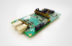
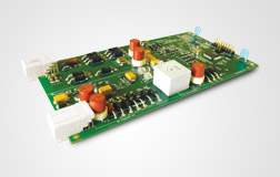
Printed Circuit boards are physical and electrical scaffolds that hold the electronics together and designing them requires a lot finesse and ingenuity. Our team of experienced engineers work closely with customers to design reliable, cost effective and rugged circuit boards considering various points:
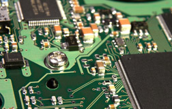
- Implemented Foundation Fieldbus connectivity.
- Scope of work : Feasibility study, Schematic design, PCB Design, Prototype development and testing, Firmware development and testing.
- Atmel ARM microcontroller, Renesas M16C/62 series microcontroller.
- Pulled off an extremely complex 16 layered PCB design task of assembling all components required for Foundation Fieldbus within Intrinsic Safety norms (large clearances) while having to maintain the board size.
- Which is the most suitable laminate material, layer and thickness configuration considering electrical and mechanical requirements and cost?
- Which is the most optimal component placement strategy in regards to thermal performance, signal integrity, mechanical strength, manufacturability, testing and cost?
- What is the most appropriate signal routing, ground plane design and shielding strategy for carrying sensitive micro-power signals?
- How can we optimize the board layers, and parameters such as minimum clearances and via types to control yield, cost and signal performance?
- How do we minimize effect of parasitic track inductances in high power switching circuits and ensure reliability?
- What is the best placement and routing strategy for systems with multiple intrinsically safe regions?
- Simulating at an early stage as to how the component heights, cable entry paths, buttons access, displays, jumpers etc. agree well with the enclosure, to minimize re-spins.
- Simulating crosstalk, emissions and signal quality in high speed designs.
- How can we improve routing and signal quality by swapping GPIO pins on MCUs and FPGAs?
If the need arises, we work closely with reputable Printed Circuit Board fabrication houses to qualify designs for DFM. Our key differentiator is our rigorous, proprietary design and review process that ensures reliable result in minimal time.
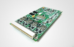
- To develop a prototype of an innovative metering device having very high SMT component density.
- Scope of work:
- Component procurement
- Component assembly using automatic pick and place machine
- Visual inspection of boards for quality control
- Used high tech Automatic Pick & Place machines and Reflow Solder for PCB assembly.
Prototyping
PCB testing services are offered optionally in conjunction with layout design.We use a combination of automatic and semi-automatic tools or hand placement as per need dictated by PCB design and density, component types and sizes to create clean-cut protos suitable for immediate testing. The same engineers who may have created PCB layout design work side-by-side with prototyping technicians as an advantage. The following points are considered:
- ESD Safe environment, component handling and packaging
- Components purchased from only the most reputable suppliers
- Individual discrete are tested immediately before placement to rule out supplier tagging error
- In-house semi-automatic SMT line ensures no communication delays
- Visual inspection of finished boards
- µBGA x-ray inspection (provided by our partners)
- Reworking using state-of-the-art tools and techniques
- Conformal coating and epoxy potting/encapsulation
- Rigorous procedural methods ensure reliable results
Design Capabilities
- Multilayer rigid, flex and rigid-flex boards
- Mixed signal, low and high power boards
- µBGA breakout and routing
- High speed designs upto 2 GHz
- Large in-house CAD library
- Designs as per IPC Standards
- Backplane design
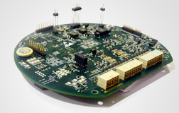
- Ultrasonic meter for measurement of Biogas, Compressed air, Natural gas, Propane, Butane, Nitrogen & Oxygen.
- Actel FPGA & Freescale K60/ARM Cortex-M4 based design.
- Low power, 12 layer board comprising 4 BGAs and Intrinsically Safe zones/power supply.
- UART, USB, HART based communication.
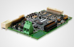
- FPGA based design.
- Intrinsically safe power supply.
- Intrinsically safe zones.
- Scope of work: Printed Circuit Board layout, Component procurement, Prototype development, Testing
- Engagement : Offsite, 20 weeks
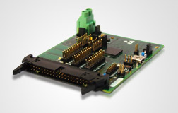
- Developed for a low-power Microcontroller family.
- Capacitive touchpad.
- Scope of work: PCB layout, Component procurement, Prototype development, Testing
- Engagement : Offsite, 20 weeks


