
Home > PCB Engineering
Build High-Performance Electronic Products with End-to-End PCB Engineering
At Ascenten Technologies, we help businesses transform electronic concepts into reliable, production-ready products through comprehensive PCB Engineering Services. Our engineering team combines practical experience with advanced design methodologies to develop printed circuit boards that meet demanding technical and commercial requirements.
From PCB Layout and Design to Stack-up, Simulation, Prototyping, and manufacturing support, we provide end-to-end Electronic Product Design services tailored to a wide range of applications. We design solutions for industrial automation, medical devices, automotive electronics, consumer products, and IoT applications, ensuring every design delivers optimal performance, streamlined manufacturability, and long-term reliability.
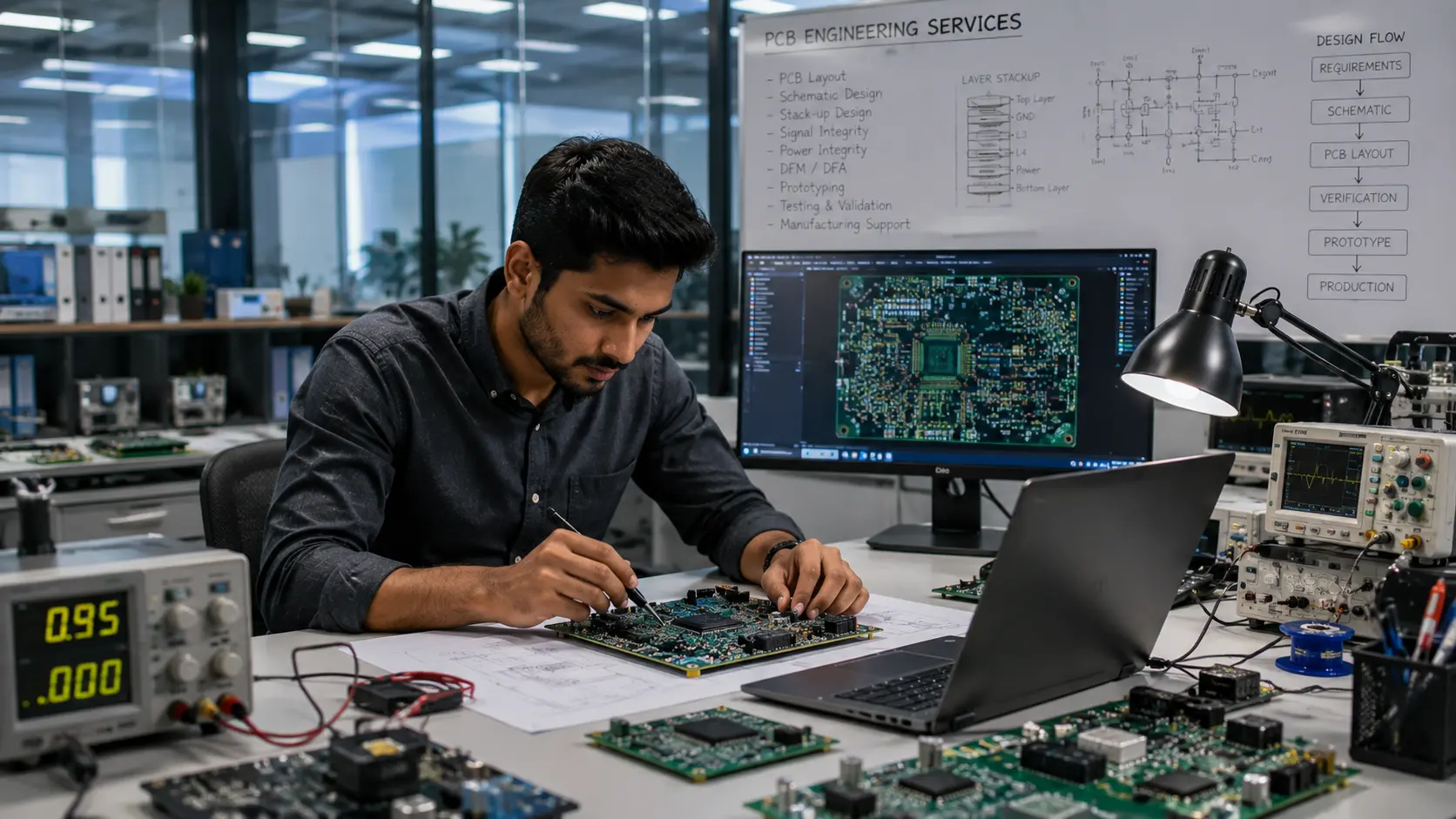
Our structured engineering process helps to minimize the development risks, shorten product development cycles and prepare hardware for successful production.
Every electronic product has its own design challenges. Our engineers help you through every stage of the PCB design process and can help create design documents for reliable manufacturing, from the initial schematics to final production.
Every engagement is backed by deep technical knowledge, proven methodologies, and a commitment to delivering robust and reliable products.
A well-designed PCB layout is crucial for maintaining electrical performance, thermal efficiency and manufacturing quality. Our engineers develop optimized layouts that satisfy electrical, mechanical and production requirements while minimizing design risks.
Every layout is engineered to improve signal integrity, simplify manufacturing, and support long-term product reliability.
Our capabilities include:
A successful electronic product starts with a robust circuit architecture. Our engineers create efficient PCB designs that balance functionality, power consumption, reliability, and production requirements.
Each design undergoes engineering reviews throughout development to reduce redesign efforts and improve manufacturing readiness.
Our services include:
The layer structure of a PCB directly influences signal quality, thermal management, manufacturing consistency and overall product performance. Our engineers optimize stack-up configurations to ensure stable electrical performance and reliable production.
Proper stack-up planning from the start reduces costly revisions and contributes to consistent production quality.
Our stack-up engineering covers:
Before a board goes into fabrication, simulation identifies potential issues that are far more expensive to fix after the fact. Our engineers use industry-standard tools to validate designs for signal integrity, power integrity, and thermal performance.
Simulation-driven design minimizes prototype iterations and accelerates time-to-market.
Our simulation capabilities include:
Getting a design production-ready requires more than a finished PCB layout. Our engineering team provides manufacturing support that bridges design completion and successful production.
This support ensures a smooth handover to manufacturing and reduces first-article failures.
Our manufacturing support includes:
Rapid prototyping is a process that links design and production. As one of the trusted prototyping service providers, our PCB prototype design services allow teams to test hardware performance, identify design improvements early, and iterate quickly before committing to volume manufacturing.
We iterate efficiently so clients can reduce development costs and move toward production with confidence.
Our prototyping services include:
Our PCB engineering experience spans a broad range of industries and product categories. We have designed boards for applications requiring precision, durability, and compliance with industry-specific standards.
Each industry brings its own regulatory requirements and performance expectations. Our engineers design with those constraints in mind from day one.
Industries we serve:
Selecting the right engineering partner is important. As a trusted hardware product design company, Ascenten Technologies combines deep PCB engineering expertise with practical manufacturing knowledge to ensure that boards perform reliably in production.
Experienced PCB engineering team with domain-specific expertise.
Complete PCB design services from schematic to manufacturing documentation.
End-to-end support across layout, stack-up, simulation, and prototyping.
Proven hardware product design services across multiple industries.
DFM and DFA practices built into every project.
Faster prototype development and iteration cycles.
Scalable manufacturing support for volume production.
Dedicated engineering team with clear project communication.
Our engineers are happy to work with you to ensure that, from a technical, commercial and production standpoint, we are able to provide a solution that will meet your requirements, whether you are designing a new electronic product or redesigning an existing board.
Start Your Project
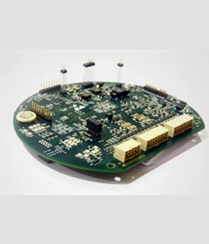
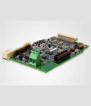
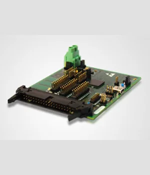
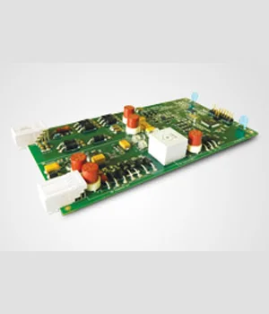
From initial concept to production-ready hardware, Ascenten Technologies delivers PCB engineering solutions that power reliable electronic products.
Whether you need custom hardware design services, dedicated PCB design services, rapid prototyping, or complete turnkey electronics product development, our team is ready to help you build smarter and faster.
We would really like to hear from you and answer any questions. Please email us at info1@ascenten.net
or call us on
India Landline: +91-79-2646 4646
India Mobile: +91-89800 00973
Home | Careers | Ethics | Privacy Policy | Terms Of Use | Code Of Conduct